Our mission
Accelerating next-gen technologies by unlocking the potential of diamond.
Our mission at staC12 is to accelerate next-gen technologies by unlocking the potential of diamond through the best-in-class thin film diamond integration.
- Thin film
- Extremely thin diamonds with controllable thickness, allowing for seamless integration
- Single crystal
- One piece of diamond, rather than pieces of diamond joined together
- Isotopically purified
- Only one carbon isotope present in the diamond (C12), creating the highest quality diamonds
Product
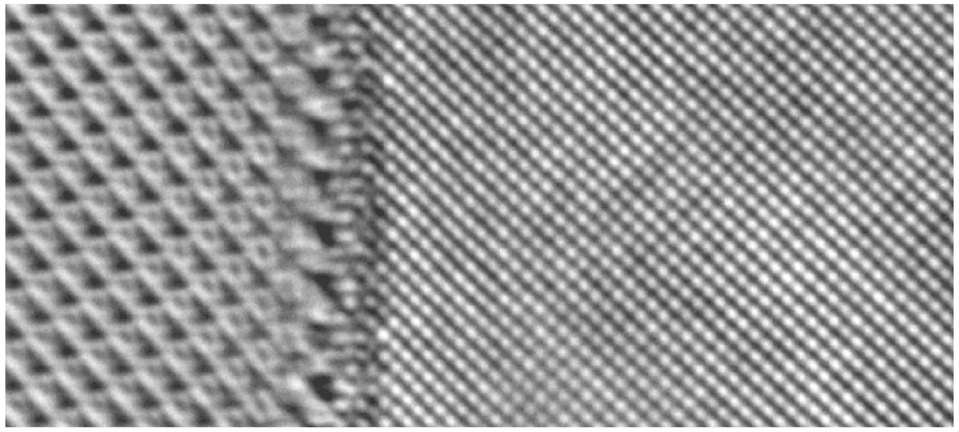
We provide bonded thin-film diamond that’s single crystal, isotopically purified, and custom for your application.
The single crystal diamond advantage
| Property | Silicon (Si) | Diamond (C) |
|---|---|---|
| Bandgap energy | 1.12 eV | 5.47eV |
| Thermal conductivity | ~150 W/m·K | >3,000W/m·K |
| Electron mobility | 1,450 cm²/V·s | 2,200cm²/V·s |
| Physical hardness | ~7 Mohs | 10Mohs |
Plus
- Room temperature quantum operation
- Wide band-gap
- Sub-nanometer surfaces
- Highest radiation tolerance
And more.
Applications
Our integrated diamond material enables breakthrough capabilities across technologies.


Industry feedback
Industry leaders are excited about our integrated diamond material across numerous applications. Here’s what some have said:
“How soon can you get me diamond on silicon?”
“When can we buy one?”
“Ideally, I would buy [from you] tomorrow.”